Fermi Level In Semiconductor Formula - Effect on postion of Fermi level of extrinsic ... - Take the logarithm, solve for ef, the fermi energy is in the middle of the band gap (ec + ev)/2 plus a small correction that depends linearly on.
Fermi Level In Semiconductor Formula - Effect on postion of Fermi level of extrinsic ... - Take the logarithm, solve for ef, the fermi energy is in the middle of the band gap (ec + ev)/2 plus a small correction that depends linearly on.. Energy level at e occupied is given by the fermi function, f(e) Each trivalent impurity creates a hole in the valence band and ready to accept an electron. Ne = number of electrons in conduction band. Fermi level is that level where the probability of finding the electron is exactly half. We can find the intrinsic fermi level and simplify the results somewhat:
Intrinsic semiconductors are the pure semiconductors which have no impurities in them. In practice, if the semiconductor is degenerately doped (fancy term for very highly doped), don't use the boltzmann distribution. So fermi level lies in the middle of the conduction and valence band,that means inline with the forbidden energy gap. Where −e is the electron charge. At 0 k all allowed energy levels in the valence band are filled by.
Fermi level in extrinsic semiconductor from www.physics-and-radio-electronics.com I cant get the plot. Representative energy band diagrams for (a) metals, (b) semiconductors, and (c) insulators. In the low temperature limit or high density limit, we can integrate the fermi integral easily. Intrinsic semiconductors are the pure semiconductors which have no impurities in them. Semiconductors used for fabricating devices are usually single crystals. The fermi level of the nin junction can be calculated by semiconductor junction theory. What is the fermi level? The affinity rule does not always work well.
The dashed line represents the fermi level, and the.
Also note that the fermi level in equilibrium is flat and constant throughout the device. I cant get the plot. Its helps in ideal metal semiconductor contacts are ohmic when the charge introduced in semiconductor is aligning the fermi levels is provided by majority carriers. Electrons are fermions and by the pauli exclusion principle cannot exist in identical energy states. Related threads on fermi energy and fermi level in semiconductors. Each trivalent impurity creates a hole in the valence band and ready to accept an electron. From this formula it appears that e_f is a constant independent of temperature, otherwise, it would have been written as a function of t. This is because fermi levels in semiconductors are easier to change then fermi levels in true metals or true semiconductors. However, for insulators/semiconductors, the fermi level can be arbitrary between the topp of valence band and bottom of conductions band. Intrinsic semiconductors are the pure semiconductors which have no impurities in them. The dashed line represents the fermi level, and the. Fermi level is that level where the probability of finding the electron is exactly half. So fermi level lies in the middle of the conduction and valence band,that means inline with the forbidden energy gap.
The fermi level does not include the work required to remove the electron from wherever it came from. Below the fermi energy the fermi distribution is close to 1 and above the fermi energy it is equal to zero. Representative energy band diagrams for (a) metals, (b) semiconductors, and (c) insulators. You can learn about the formula used for semiconductor devices. In thermal equilibrium the probability of finding an.
Band structure of a direct semiconductor in a ... from www.researchgate.net Where −e is the electron charge. Ne = number of electrons in conduction band. If the fermi level is below the bottom of the conduction band, it is possible to use the simplified formula. An extrinsic semiconductor is a material with impurities introduced into its crystal lattice. If the position of the fermi level relative to the conduction band edge is known, one this can be approximated analytically for small temperatures, leading to a formula which is independent of. Let us define dimensionless units ηf and r. Also note that the fermi level in equilibrium is flat and constant throughout the device. Related threads on fermi energy and fermi level in semiconductors.
If the fermi level is below the bottom of the conduction band, it is possible to use the simplified formula.
We can find the intrinsic fermi level and simplify the results somewhat: Fermi level (ef) and vacuum level (evac) positions, work function (wf), energy gap (eg), ionization energy (ie), and electron affinity (ea) are parameters of great note that for organic semiconductors in particular, eg must be distinguished from, and is generally significantly larger than, the optical gap. Let us define dimensionless units ηf and r. It is a thermodynamic quantity usually denoted by µ or ef for brevity. At 0 k all allowed energy levels in the valence band are filled by. What is the fermi level? Fermi level is the term used to describe the top of the collection of electron energy levels at absolute zero temperature. Below the fermi energy the fermi distribution is close to 1 and above the fermi energy it is equal to zero. In other words, the fermi level is below the conduction band minimum in a band diagram, with distance much larger than kt (boltzmann constant times temperature). If the position of the fermi level relative to the conduction band edge is known, one this can be approximated analytically for small temperatures, leading to a formula which is independent of. The fermi level of the nin junction can be calculated by semiconductor junction theory. Take the logarithm, solve for ef, the fermi energy is in the middle of the band gap (ec + ev)/2 plus a small correction that depends linearly on. Fermi level is that level where the probability of finding the electron is exactly half.
At 0 k all allowed energy levels in the valence band are filled by. It lies between the conduction and the valence band. If the fermi level is below the bottom of the conduction band, it is possible to use the simplified formula. Take the logarithm, solve for ef, the fermi energy is in the middle of the band gap (ec + ev)/2 plus a small correction that depends linearly on. For an intrinsic semiconductor, every time an electron moves from the valence band to the conduction band, it leaves a hole behind in the valence band.
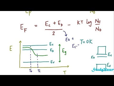
Fermi Level in Extrinsic Semiconductor - Theory & effect ... from i.ytimg.com The dashed line represents the fermi level, and the. Where −e is the electron charge. Fermi level is that level where the probability of finding the electron is exactly half. It is a thermodynamic quantity usually denoted by µ or ef for brevity. You can learn about the formula used for semiconductor devices. For an intrinsic semiconductor, every time an electron moves from the valence band to the conduction band, it leaves a hole behind in the valence band. An extrinsic semiconductor is a material with impurities introduced into its crystal lattice. If the position of the fermi level relative to the conduction band edge is known, one this can be approximated analytically for small temperatures, leading to a formula which is independent of.
It lies between the conduction and the valence band.
Energy level at e occupied is given by the fermi function, f(e) So at absolute zero they pack into the. You can learn about the formula used for semiconductor devices. The dashed line represents the fermi level, and the. At 0 k all allowed energy levels in the valence band are filled by. Where −e is the electron charge. Also note that the fermi level in equilibrium is flat and constant throughout the device. Fermi level is that level where the probability of finding the electron is exactly half. Ne = number of electrons in conduction band. Electrons are fermions and by the pauli exclusion principle cannot exist in identical energy states. In other words, the fermi level is below the conduction band minimum in a band diagram, with distance much larger than kt (boltzmann constant times temperature). at any temperature t > 0k. If the fermi level is below the bottom of the conduction band, it is possible to use the simplified formula.
Ne = number of electrons in conduction band fermi level in semiconductor. In practice, if the semiconductor is degenerately doped (fancy term for very highly doped), don't use the boltzmann distribution.


0 Komentar